

正確な見積もりを受け取るには、製品の詳細(色、サイズ、素材など)やその他の具体的な要件を入力してください。
伝言を残す
弊社製品にご興味をお持ちで、さらに詳しい情報をご希望の場合は、こちらにメッセージを残してください。できる限り早くご返信いたします。
他の

製品


Semiconductor Manufacturing & Packaging Equipment

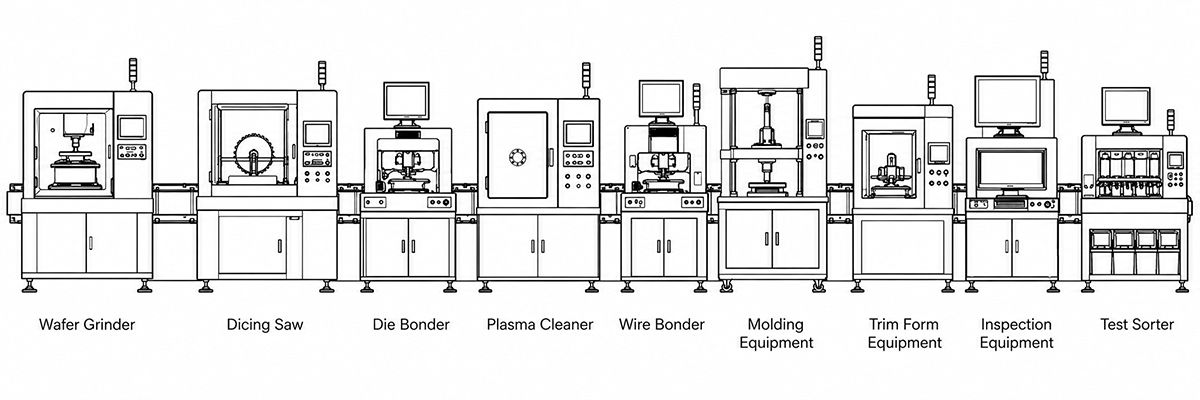
HYRNUS provides semiconductor manufacturing, packaging and testing equipment for research, pilot production and mass-production applications. Our equipment portfolio covers multiple processes from wafer preparation and die attachment to wire bonding, molding, inspection, testing and final sorting.

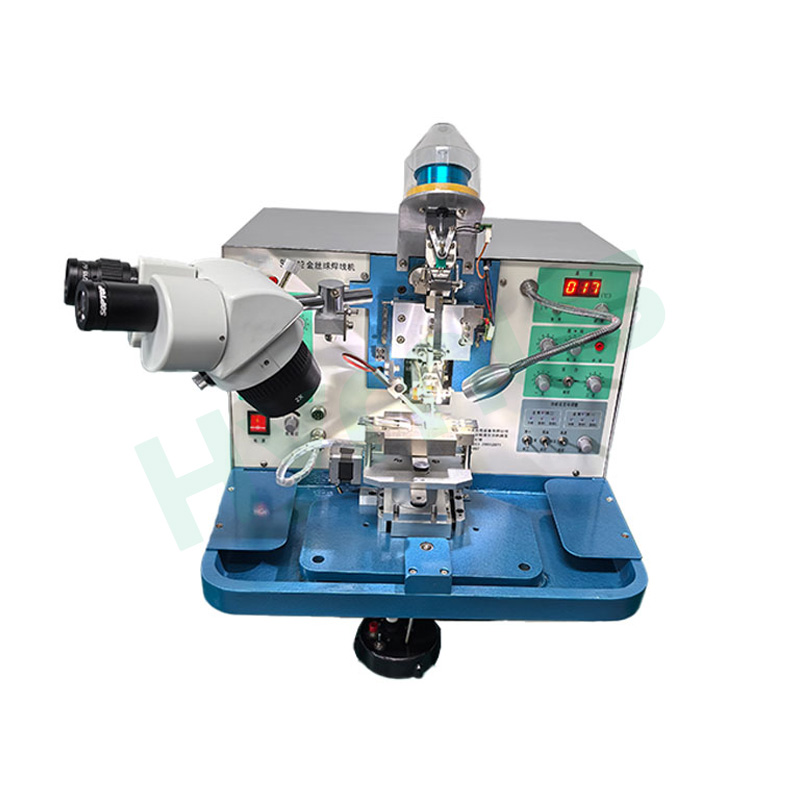
  • Gold Wire Bonder
    金線ボンディングボールボンディングマシン
    HY-GB2012金ボールワイヤボンダーは、主に高出力LED、レーザーダイオード、中小出力ダイオード、トランジスタ、集積回路、センサー、特殊半導体デバイスの内部リードボンディングに使用されます。特に高出力LEDデバイスのワイヤボンディングに適しています。
    続きを読む
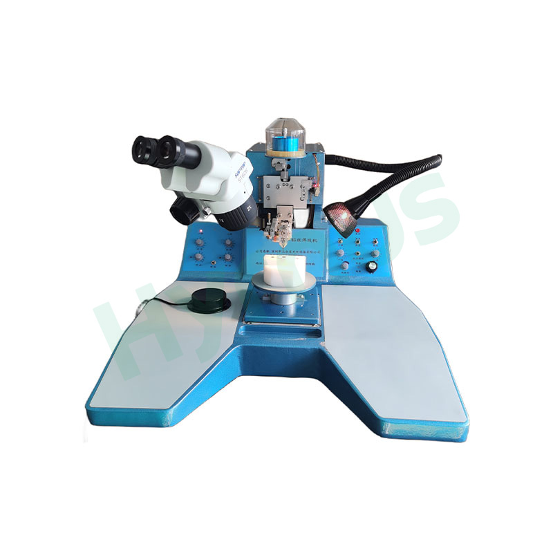
  • wedge bonding machine
    実験室用超音波ワイヤボンディング装置
    HY-WB2000超音波ワイヤボンダーは、細いアルミ線、圧力、および超音波エネルギーを用いて、チップと基板間の信頼性の高い電気接続を実現します。マイクロ波デバイス、RFモジュール、ハイブリッド回路、MEMS、光電子デバイス、センサー、半導体デバイス、レーダーデバイス、COB/SOBパッケージング、その他マイクロエレクトロニクス用途に適しています。
    続きを読む


One-Stop Semiconductor Equipment Solutions

In addition to standalone semiconductor equipment, HYRNUS provides equipment configuration and integrated production line solutions for semiconductor manufacturing and electronic component packaging.


Get A custom solution
 

01

Production Line Planning

Plan the production process, equipment layout, material flow and workstation configuration based on the available factory space, target capacity and automation requirements.


02

Process Solution Development

Develop a suitable process flow according to the device type, package structure, materials and manufacturing requirements, covering key processes such as die attach, wire bonding, molding, inspection, testing and sorting.


03

Equipment Selection and Configuration

Select and configure suitable machines based on production capacity, material compatibility, positioning accuracy, process control, automation level and data traceability requirements.

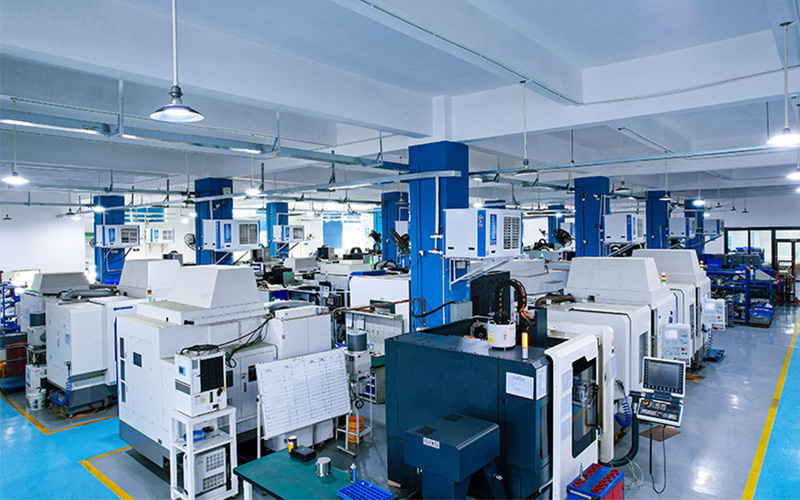
Semiconductor packaging production line

伝言を残す

伝言を残す
弊社製品にご興味をお持ちで、さらに詳しい情報をご希望の場合は、こちらにメッセージを残してください。できる限り早くご返信いたします。
お問い合わせ :allen@hyrnus.com